Esercitazione di Laboratorio
Carlo Calò
Classe
Materia
Argomento
5ª Elettronici
T.D.P.
Controllo di Potenza
Controllo di potenza in continua con transistor in commutazione
pilotato da un segnale PWM
Vogliamo costruire un circuito che ci permetta di controllare la potenza di un carico
alimentato da una batteria tramite un transistor fatto funzionare alternativamente in
conduzione e interdizione.
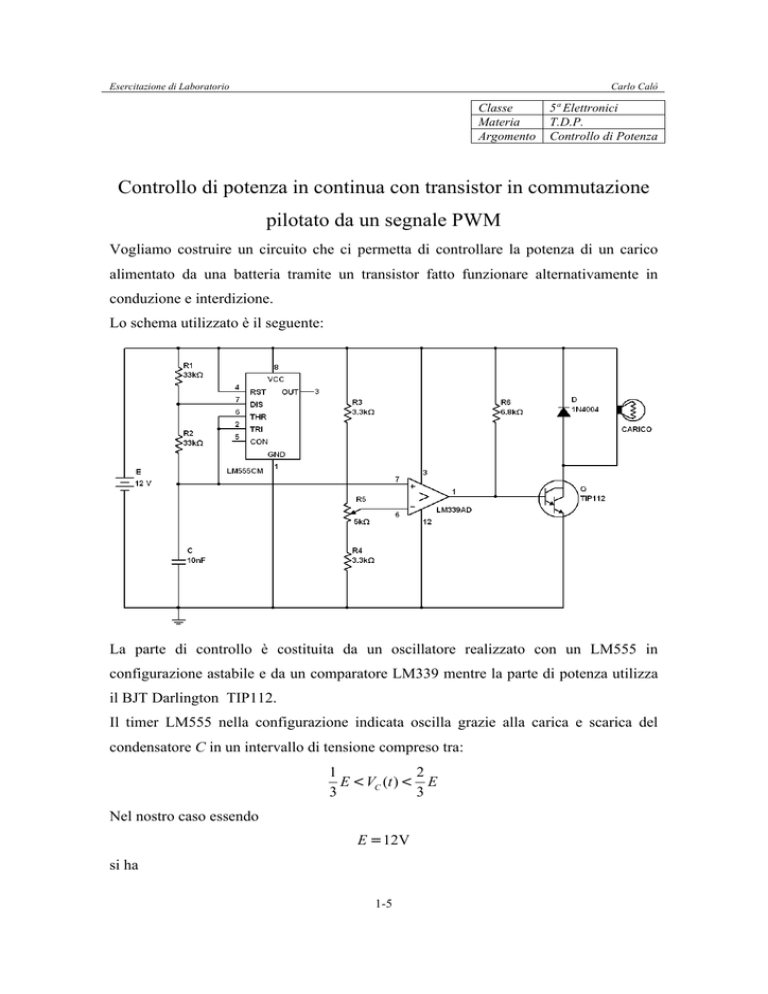
Lo schema utilizzato è il seguente:
La parte di controllo è costituita da un oscillatore realizzato con un LM555 in
configurazione astabile e da un comparatore LM339 mentre la parte di potenza utilizza
il BJT Darlington TIP112.
Il timer LM555 nella configurazione indicata oscilla grazie alla carica e scarica del
condensatore C in un intervallo di tensione compreso tra:
1
2
E < VC (t ) < E
3
3
Nel nostro caso essendo
E = 12V
si ha
1-5
Esercitazione di Laboratorio
Carlo Calò
4 < VC (t ) < 8 V
L’LM555 gestisce la carica e scarica del
condensatore rilevando la tensione ai suoi capi
grazie ai pin 6 e 2 (threshold e trigger) aprendo e
chiudendo alternativamente un interruttore al suo
interno che fa capo al pin 7 (discharge).
Nel passaggio da 4 V a 8 V il condensatore si
carica tramite la batteria attraverso le due
resistenze R1 ed R2 in un tempo T1 pari a:
T1 = ( R1 + R2 ) C log e 2
Nel passaggio da 8 V a 4 V il condensatore si scarica attraverso la sola resistenza R2 sul
piedino 7 del LM555 che si porta a massa in un tempo pari a:
T2 = R2C log e 2
Nella fase di carica il pin 3 (output) si porta a livello logico alto (12 V) mentre in quella
di scarica a livello logico basso (~0 V).
2-5
Esercitazione di Laboratorio
Carlo Calò
Nel caso in esame sul pin 3 di uscita si ha quindi un’onda rettangolare avente una
frequenza:
f=
1
1
1
1
=
=
=
≅1457Hz
3
T T1 +T2 ( R1 + 2 R2 ) C log e 2 3⋅33⋅10 ⋅10⋅10−9 ⋅log e 2
e un duty-cycle:
d.c.(%) =
T1
T
R + R2
2
= 1 = 1
= ≅ 66.7%
T T1 +T2 R1 + 2 R2 3
Il nostro obiettivo è però quello di avere un’onda rettangolare con duty-cycle variabile
in un intervallo compreso tra 0 e il 100%.
Per fare questo si usa la tensione ai capi del condensatore e la si confronta con una
tensione costante nel comparatore LM339 che in uscita darà il valore alto solo quando la
tensione al morsetto positivo supererà quella di riferimento.
La tensione di confronto all’ingresso negativo del comparatore è ottenuta tramite un
partitore costituito dalle resistenze R3 ed R4 e dal trimmer R5.
Con i valori scelti si ha:
R4
3.3⋅103
3.3
V−min =
E=
≅ 3.41< 4 = V+min
3 E = 12
(3.3+ 3.3+ 5)⋅10
R3 + R4 + R5
11.6
e
V−max =
(3.3+ 5)⋅103
R4 + R5
8.3
E=
≅ 8.59 > 8 = V+max
3 E = 12
(3.3+ 3.3+ 5)⋅10
R3 + R4 + R5
11.6
Pertanto
al
variare
del
trimmer,
la
tensione
sull’ingresso negativo varia in un intervallo più ampio
rispetto a quella del condensatore che è limitata tra 4 e
8 V.
Le figure successive mostrano l’andamento della
tensione a vuoto all’uscita del comparatore per diversi
valore di regolazione del trimmer dalla minima alla
massima
resistenza
(L’LM339
ha
un’uscita
open-collector e richiede una resistenza di pull-up).
3-5
Esercitazione di Laboratorio
Carlo Calò
4-5
Esercitazione di Laboratorio
Carlo Calò
Collegata all’uscita del comparatore vi è infine
la parte di potenza costituita da un transistor
Darlington ad elevato guadagno (valori di hFE
compresi tra 500 e 1000) ed una corrente di
collettore ICmax=2 A.
La resistenza di base del TIP112 è stata
calcolata per avere un margine di sicurezza sul
dispositivo, infatti quando il comparatore si
trova nello stato OFF si ha:
IB =
E −VBE 0 12 − 2.8
=
=1.35 mA
R6
6.8⋅103
pertanto risulta nella peggiore delle ipotesi:
I C = hFE max I B =1000⋅1.35⋅10−3 =1.35A
che è minore della massima corrente di collettore ammessa dal BJT.
Per concludere è stato inserito sul collettore del TIP112 il diodo 1N4004 che serve ad
utilizzare il circuito anche con carichi induttivi come motori in corrente continua.
Datasheets allegati:
• LM555
• LM339
• TIP112
5-5
www.fairchildsemi.com
LM555/NE555/SA555
Single Timer
Features
Description
•
•
•
•
•
The LM555/NE555/SA555 is a highly stable controller
capable of producing accurate timing pulses. With a
monostable operation, the time delay is controlled by one
external resistor and one capacitor. With an astable
operation, the frequency and duty cycle are accurately
controlled by two external resistors and one capacitor.
High Current Drive Capability (200mA)
Adjustable Duty Cycle
Temperature Stability of 0.005%/°C
Timing From µSec to Hours
Turn off Time Less Than 2µSec
Applications
•
•
•
•
8-DIP
Precision Timing
Pulse Generation
Time Delay Generation
Sequential Timing
1
8-SOP
1
Internal Block Diagram
R
GND
1
Trigger
2
R
Comp.
Output
Reset
3
OutPut
Stage
R
8
Vcc
7
Discharge
6
Threshold
5
Control
Voltage
Discharging Tr.
F/F
4
Vref
Comp.
Rev. 1.0.3
©2002 Fairchild Semiconductor Corporation
LM555/NE555/SA555
Absolute Maximum Ratings (TA = 25°
25°C)
Parameter
Value
Unit
VCC
16
V
TLEAD
300
°C
PD
600
mW
Operating Temperature Range
LM555/NE555
SA555
TOPR
0 ~ +70
-40 ~ +85
°C
Storage Temperature Range
TSTG
-65 ~ +150
°C
Supply Voltage
Lead Temperature (Soldering 10sec)
Power Dissipation
2
Symbol
LM555/NE555/SA555
Electrical Characteristics
(TA = 25°C, VCC = 5 ~ 15V, unless otherwise specified)
Parameter
Symbol
Conditions
Min.
Typ.
Max.
Unit
Supply Voltage
VCC
-
4.5
-
16
V
Supply Current (Low Stable) (Note1)
ICC
VCC = 5V, RL = ∞
-
3
6
mA
VCC = 15V, RL = ∞
-
7.5
15
mA
-
1.0
50
0.1
3.0
%
ppm/°C
%/V
2.25
150
0.3
-
%
ppm/°C
%/V
Timing Error (Monostable)
Initial Accuracy (Note2)
Drift with Temperature (Note4)
Drift with Supply Voltage (Note4)
Timing Error (Astable)
Intial Accuracy (Note2)
Drift with Temperature (Note4)
Drift with Supply Voltage (Note4)
ACCUR
∆t/∆T
∆t/∆VCC
ACCUR
∆t/∆T
∆t/∆VCC
RA = 1kΩ to100kΩ
C = 0.1µF
RA = 1kΩ to 100kΩ
C = 0.1µF
VCC = 15V
9.0
10.0
11.0
V
VCC = 5V
2.6
3.33
4.0
V
VCC = 15V
-
10.0
-
V
VCC = 5V
-
3.33
-
V
-
0.1
0.25
µA
VCC = 5V
1.1
1.67
2.2
V
VCC = 15V
4.5
Control Voltage
VC
Threshold Voltage
VTH
Threshold Current (Note3)
ITH
Trigger Voltage
VTR
Trigger Current
ITR
Reset Voltage
VRST
-
Reset Current
IRST
-
Low Output Voltage
High Output Voltage
VOL
VOH
-
0.5
-
VTR = 0V
0.4
5
5.6
V
0.01
2.0
µA
0.7
1.0
V
0.1
0.4
mA
VCC = 15V
ISINK = 10mA
ISINK = 50mA
-
0.06
0.3
0.25
0.75
V
V
VCC = 5V
ISINK = 5mA
-
0.05
0.35
V
12.5
13.3
-
12.75
V
V
2.75
3.3
-
V
VCC = 15V
ISOURCE = 200mA
ISOURCE = 100mA
VCC = 5V
ISOURCE = 100mA
Rise Time of Output (Note4)
tR
-
-
100
-
ns
Fall Time of Output (Note4)
tF
-
-
100
-
ns
Discharge Leakage Current
ILKG
-
-
20
100
nA
Notes:
1. When the output is high, the supply current is typically 1mA less than at VCC = 5V.
2. Tested at VCC = 5.0V and VCC = 15V.
3. This will determine the maximum value of RA + RB for 15V operation, the max. total R = 20MΩ, and for 5V operation, the max.
total R = 6.7MΩ.
4. These parameters, although guaranteed, are not 100% tested in production.
3
LM555/NE555/SA555
Application Information
Table 1 below is the basic operating table of 555 timer:
Table 1. Basic Operating Table
Threshold Voltage
Trigger Voltage
Discharging Tr.
Reset(PIN 4)
Output(PIN 3)
(Vth)(PIN 6)
(Vtr)(PIN 2)
(PIN 7)
Don't care
Don't care
Low
Low
ON
Vth > 2Vcc / 3
High
Low
ON
Vth > 2Vcc / 3
High
Vcc / 3 < Vth < 2 Vcc / 3 Vcc / 3 < Vth < 2 Vcc / 3
Vth < Vcc / 3
High
High
OFF
Vth < Vcc / 3
When the low signal input is applied to the reset terminal, the timer output remains low regardless of the threshold voltage or
the trigger voltage. Only when the high signal is applied to the reset terminal, the timer's output changes according to
threshold voltage and trigger voltage.
When the threshold voltage exceeds 2/3 of the supply voltage while the timer output is high, the timer's internal discharge Tr.
turns on, lowering the threshold voltage to below 1/3 of the supply voltage. During this time, the timer output is maintained
low. Later, if a low signal is applied to the trigger voltage so that it becomes 1/3 of the supply voltage, the timer's internal
discharge Tr. turns off, increasing the threshold voltage and driving the timer output again at high.
1. Monostable Operation
+Vcc
2
10
THRES
3
6
OUT
C1
GND
CONT 5
1
Ω
10
M
Ω
1M
10
0k
Ω
R
TRIG
Capacitance(uF)
2
RL
1
10
DISCH 7
10
kΩ
Trigger
=1
kΩ
8
Vcc
AA
4
RESET
RA
0
10
-1
10
-2
10
C2
-3
10
-5
10
-4
10
-3
10
-2
10
-1
10
0
10
1
10
Time Delay(s)
Figure 1. Monoatable Circuit
Figure 3. Waveforms of Monostable Operation
4
Figure 2. Resistance and Capacitance vs.
Time delay(td)
2
10
LM555/NE555/SA555
Figure 1 illustrates a monostable circuit. In this mode, the timer generates a fixed pulse whenever the trigger voltage falls
below Vcc/3. When the trigger pulse voltage applied to the #2 pin falls below Vcc/3 while the timer output is low, the timer's
internal flip-flop turns the discharging Tr. off and causes the timer output to become high by charging the external capacitor C1
and setting the flip-flop output at the same time.
The voltage across the external capacitor C1, VC1 increases exponentially with the time constant t=RA*C and reaches 2Vcc/3
at td=1.1RA*C. Hence, capacitor C1 is charged through resistor RA. The greater the time constant RAC, the longer it takes
for the VC1 to reach 2Vcc/3. In other words, the time constant RAC controls the output pulse width.
When the applied voltage to the capacitor C1 reaches 2Vcc/3, the comparator on the trigger terminal resets the flip-flop,
turning the discharging Tr. on. At this time, C1 begins to discharge and the timer output converts to low.
In this way, the timer operating in the monostable repeats the above process. Figure 2 shows the time constant relationship
based on RA and C. Figure 3 shows the general waveforms during the monostable operation.
It must be noted that, for a normal operation, the trigger pulse voltage needs to maintain a minimum of Vcc/3 before the timer
output turns low. That is, although the output remains unaffected even if a different trigger pulse is applied while the output is
high, it may be affected and the waveform does not operate properly if the trigger pulse voltage at the end of the output pulse
remains at below Vcc/3. Figure 4 shows such a timer output abnormality.
Figure 4. Waveforms of Monostable Operation (abnormal)
2. Astable Operation
+Vcc
100
RA
GND
RL
Ω
C1
Ω
OUT
0.1
M
10
3
1
1M
RB
THRES 6
Capacitance(uF)
7
TRIG
Ω
0k
10
DISCH
2
10
Ω
1k
8
Vcc
kΩ
10
4
RESET
(R A+2R B)
0.01
CONT 5
1
C2
1E-3
100m
1
10
100
1k
10k
100k
Fr equency(Hz)
Figure 5. Astable Circuit
Figure 6. Capacitance and Resistance vs. Frequency
5
LM555/NE555/SA555
Figure 7. Waveforms of Astable Operation
An astable timer operation is achieved by adding resistor RB to Figure 1 and configuring as shown on Figure 5. In the astable
operation, the trigger terminal and the threshold terminal are connected so that a self-trigger is formed, operating as a multi
vibrator. When the timer output is high, its internal discharging Tr. turns off and the VC1 increases by exponential
function with the time constant (RA+RB)*C.
When the VC1, or the threshold voltage, reaches 2Vcc/3, the comparator output on the trigger terminal becomes high,
resetting the F/F and causing the timer output to become low. This in turn turns on the discharging Tr. and the C1 discharges
through the discharging channel formed by RB and the discharging Tr. When the VC1 falls below Vcc/3, the comparator
output on the trigger terminal becomes high and the timer output becomes high again. The discharging Tr. turns off and the
VC1 rises again.
In the above process, the section where the timer output is high is the time it takes for the VC1 to rise from Vcc/3 to 2Vcc/3,
and the section where the timer output is low is the time it takes for the VC1 to drop from 2Vcc/3 to Vcc/3. When timer output
is high, the equivalent circuit for charging capacitor C1 is as follows:
RA
RB
Vcc
C1
dv c1 V cc – V ( 0- )
C ------------- = ------------------------------1 dt
RA + RB
V
C1
( 0+ ) = V
CC
⁄3
Vc1(0-)=Vcc/3
(1)
(2)
t
- – ------------------------------------
( R + R )C1
2 A B
V C1 ( t ) = V CC 1 – --- e
3
(3)
Since the duration of the timer output high state(tH) is the amount of time it takes for the VC1(t) to reach 2Vcc/3,
6
LM555/NE555/SA555
t
H
- – ------------------------------------
2
2 ( R A + R B )C1
V ( t ) = --- V
=V
1 – --- e
C1
3 CC
3
CC
t
H
(4)
(5)
= C ( R + R )In2 = 0.693 ( R + R )C
A
B 1
1 A
B
The equivalent circuit for discharging capacitor C1, when timer output is low is, as follows:
RB
C1
VC1(0-)=2Vcc/3
RD
dv
1
C1
C 1 -------------- + ----------------------- V C1 = 0
R +R
dt
A
B
2
V C1 ( t ) = --- V
3 CC e
t
- ------------------------------------( R A + R D )C1
(6)
(7)
Since the duration of the timer output low state(tL) is the amount of time it takes for the VC1(t) to reach Vcc/3,
tL
- -----------------------------------( R A + R D )C1
1
2
--- V
-= V
(8)
3 CC 3 CC e
t = C ( R + R )In2 = 0.693 ( R + R )C
B
D 1
L
1 B
D
(9)
Since RD is normally RB>>RD although related to the size of discharging Tr.,
(10)
tL=0.693RBC1
Consequently, if the timer operates in astable, the period is the same with
'T=tH+tL=0.693(RA+RB)C1+0.693RBC1=0.693(RA+2RB)C1' because the period is the sum of the charge time and discharge
time. And since frequency is the reciprocal of the period, the following applies.
frequency,
1
1.44
f = --- = ---------------------------------------T
( R + 2R )C
A
B 1
( 11 )
3. Frequency divider
By adjusting the length of the timing cycle, the basic circuit of Figure 1 can be made to operate as a frequency divider. Figure
8. illustrates a divide-by-three circuit that makes use of the fact that retriggering cannot occur during the timing cycle.
7
LM555/NE555/SA555
Figure 8. Waveforms of Frequency Divider Operation
4. Pulse Width Modulation
The timer output waveform may be changed by modulating the control voltage applied to the timer's pin 5 and changing the
reference of the timer's internal comparators. Figure 9 illustrates the pulse width modulation circuit.
When the continuous trigger pulse train is applied in the monostable mode, the timer output width is modulated according to
the signal applied to the control terminal. Sine wave as well as other waveforms may be applied as a signal to the control
terminal. Figure 10 shows the example of pulse width modulation waveform.
+Vcc
4
RA
8
RESET
Vcc
Trigger
7
DISCH
2
TRIG
6
THRES
Output
3
OUT
Input
GND
CONT
5
C
1
Figure 9. Circuit for Pulse Width Modulation
Figure 10. Waveforms of Pulse Width Modulation
5. Pulse Position Modulation
If the modulating signal is applied to the control terminal while the timer is connected for the astable operation as in Figure 11,
the timer becomes a pulse position modulator.
In the pulse position modulator, the reference of the timer's internal comparators is modulated which in turn modulates the
timer output according to the modulation signal applied to the control terminal.
Figure 12 illustrates a sine wave for modulation signal and the resulting output pulse position modulation : however, any wave
shape could be used.
8
LM555/NE555/SA555
+Vcc
4
RA
8
RESET
Vcc
7
DISCH
2
TRIG
RB
6
THRES
Output
3
OUT
Modulation
GND
5
CONT
C
1
Figure 12. Waveforms of pulse position modulation
Figure 11. Circuit for Pulse Position Modulation
6. Linear Ramp
When the pull-up resistor RA in the monostable circuit shown in Figure 1 is replaced with constant current source, the VC1
increases linearly, generating a linear ramp. Figure 13 shows the linear ramp generating circuit and Figure 14 illustrates the
generated linear ramp waveforms.
+Vcc
RE
2
4
8
RESET
Vcc
DISCH
7
THRES
6
R1
Q1
TRIG
R2
Output
3
OUT
GND
C1
CONT 5
C2
1
Figure 13. Circuit for Linear Ramp
Figure 14. Waveforms of Linear Ramp
In Figure 13, current source is created by PNP transistor Q1 and resistor R1, R2, and RE.
I
V
E
V
–V
CC
E= -------------------------C
R
E
Here, V
E is
= V
BE
R2
+ ---------------------- V
R 1 + R 2 CC
( 12 )
( 13 )
For example, if Vcc=15V, RE=20kΩ, R1=5kW, R2=10kΩ, and VBE=0.7V,
VE=0.7V+10V=10.7V
Ic=(15-10.7)/20k=0.215mA
9
LM555/NE555/SA555
When the trigger starts in a timer configured as shown in Figure 13, the current flowing through capacitor C1 becomes a
constant current generated by PNP transistor and resistors.
Hence, the VC is a linear ramp function as shown in Figure 14. The gradient S of the linear ramp function is defined as
follows:
Vp – p
S = ---------------T
( 14 )
Here the Vp-p is the peak-to-peak voltage.
If the electric charge amount accumulated in the capacitor is divided by the capacitance, the VC comes out as follows:
V=Q/C
(15)
The above equation divided on both sides by T gives us
V
Q⁄T
---- = -----------T
C
( 16 )
and may be simplified into the following equation.
S=I/C
(17)
In other words, the gradient of the linear ramp function appearing across the capacitor can be obtained by using the constant
current flowing through the capacitor.
If the constant current flow through the capacitor is 0.215mA and the capacitance is 0.02µF, the gradient of the ramp function
at both ends of the capacitor is S = 0.215m/0.022µ = 9.77V/ms.
10
LM555/NE555/SA555
Mechanical Dimensions
Package
Dimensions in millimeters
0.060 ±0.004
#5
1.524 ±0.10
#4
0.018 ±0.004
#8
2.54
0.100
9.60
MAX
0.378
#1
9.20 ±0.20
0.362 ±0.008
(
6.40 ±0.20
0.252 ±0.008
0.46 ±0.10
0.79
)
0.031
8-DIP
5.08
MAX
0.200
7.62
0.300
3.40 ±0.20
0.134 ±0.008
3.30 ±0.30
0.130 ±0.012
0.33
0.013 MIN
+0.10
0.25 –0.05
+0.004
0~15°
0.010 –0.002
11
LM555/NE555/SA555
Mechanical Dimensions (Continued)
Package
Dimensions in millimeters
8-SOP
MIN
#5
12
0~
8°
+0.10
0.15 -0.05
+0.004
0.006 -0.002
3.95 ±0.20
0.156 ±0.008
5.72
0.225
0.50 ±0.20
0.020 ±0.008
1.80
MAX
0.071
MAX0.10
MAX0.004
6.00 ±0.30
0.236 ±0.012
0.41 ±0.10
0.016 ±0.004
#4
1.27
0.050
#8
5.13
MAX
0.202
#1
4.92 ±0.20
0.194 ±0.008
(
0.56
)
0.022
1.55 ±0.20
0.061 ±0.008
0.1~0.25
0.004~0.001
www.fairchildsemi.com
LM2901,LM339/LM339A,LM3302,
LM239/LM239A
Quad Comparator
Features
Description
• Single or dual supply operation
• Wide range of supply voltage
LM2901,LM339/LM339A,LM239/LM239A : 2 ~ 36V
(or ±1 ~ ±18V)
LM3302 : 2 ~ 28V (or ±1 ~ ±14V)
• Low supply current drain 800µA Typ.
• Open collector outputs for wired and connectors
• Low input bias current 25nA Typ.
• Low Input offset current ±2.3nA Typ.
• Low input offset voltage ±1.4mV Typ.
• Common mode input voltage range includes ground.
• Low output saturation voltage
• Output compatible with TTL. DTL and MOS logic system
The LM2901, LM339/LM339A ,LM239/LM239A, LM3302
consist of four independent voltage comparators designed
to operate from single power supply over a wide voltage
range.
14-DIP
1
14-SOP
1
Internal Block Diagram
Rev. 1.0.1
©2001 Fairchild Semiconductor Corporation
LM2901,LM339/LM339A,LM3302, LM239/LM239A
Schematic Diagram
Absolute Maximum Ratings
Parameter
Symbol
Value
Unit
Supply Voltage
VCC
±18 or 36
V
Supply Voltage only LM3302
VCC
±14 or 28
V
Differential Input Voltage
VI(DIFF)
36
V
Differential Input Voltage only LM3302
VI(DIFF)
28
V
Input Voltage
VI
- 0.3 to +36
V
Input Voltage only LM3302
VI
- 0.3 to +28
V
Output Short Circuit to GND
-
Continuous
-
PD
570
mW
TOPR
0 ~ + 70
-40 ~ + 85
-25 ~ + 85
°C
TSTG
- 65 ~ + 150
°C
Power Dissipation
Operating Temperature
LM339/LM339A
LM2901/LM3302
LM239/LM239A
Storage Temperature
2
LM2901,LM339/LM339A,LM3302, LM239/LM239A
Electrical Characteristics
(VCC = 5V, TA = 25°C, unless otherwise specified)
Parameter
Input Offset
Voltage
Input Offset
Current
Input Bias Current
Symbol
VIO
Conditions
VO(P) =1.4V, RS =0Ω
Note 1
Min
Typ
Max
-
±1
±2
-
IIO
Note 1
IBIAS
Note 1
Input Common
Mode Voltage
Range
VI(R)
Supply Current
ICC
VCC = 5V RL = ∞
GV
VCC =15V, RL ≥ 15KΩ
(for large swing)
Voltage Gain
LM239A/LM339A
Note 1
±2.3
-
LM239/LM339
Min Typ
-
Max
±1.4
±5
±4.0
-
-
±9.0
±50
-
±2.3
±50
±150
-
-
±150
Unit
mV
nA
-
57
250
-
57
250
nA
-
-
400
-
-
400
0
-
VCC-1.5
0
-
VCC-1.5
0
-
VCC-2
0
-
VCC-2
-
1.1
2.0
-
1.1
2.0
mA
50
200
-
50
200
-
V/mV
V
Large Signal
Response Time
TLRES
VI = TTL Logic Swing
VREF = 1.4V, VRL = 5V,
RL = 5.1KΩ
-
350
-
-
350
-
ns
Response Time
TRES
VRL = 5V, RL = 5.1KΩ
-
1.4
-
-
1.4
-
µs
Output Sink
Current
ISINK
VI(-) ≥ 1V, VI(+) = 0V,
VO(P) ≤ 1.5V
6
18
-
6
18
-
mA
Output Saturation
Voltage
VSAT
VI(-) ≥ 1V, VI(+) = 0V
-
140
400
-
140
400
ISINK = 4mA
Note 1
-
700
-
VI(-) = 0V
VI(+) = 1V
VO(P) = 5V
-
0.1
-
-
0.1
-
nA
VO(P) = 30V
-
-
1.0
-
-
1.0
µA
Note 1
-
-
36
-
-
36
V
Output Leakage
Current
Io(LKG)
Differential Voltage VI(DIFF)
700
mV
Note 1.
LM339/LM339A : 0 ≤ TA ≤ +70°C
LM2901/LM3302 : -40 ≤ TA ≤ +85°C
LM239/LM239A : -25 ≤ TA ≤ +85°C
3
LM2901,LM339/LM339A,LM3302, LM239/LM239A
Electrical Characteristics (Continued)
(VCC = 5V, TA = 25°C, unless otherwise specified)
Parameter
Symbol
Input Offset Voltage
VIO
Input Offset Current
IIO
Input Bias Current
VO(P) =1.4V, RS =0Ω
Note 1
Note 1
IBIAS
Input Common
Mode Voltage
Range
VI(R)
Supply Current
ICC
Voltage Gain
GV
Note 1
LM2901
LM3302
Min
Typ
Max.
Min
Typ
Max.
-
2
7
-
2
20
-
9
15
-
-
40
-
2.3
50
-
3
100
-
50
200
-
-
300
-
57
250
-
57
250
-
200
500
-
-
1000
0
-
VCC
-1.5
0
-
VCC
-1.5
0
-
VCC
-2
Unit
mV
nA
nA
V
Note 1
0
-
VCC
-2
RL =∞, VCC=5V
-
1.1
2.0
-
1.1
2.0
RL =∞,VCC=30V
-
1.6
2.5
-
-
-
25
100
-
2
30
-
-
350
-
1.4
-
µs
mA
VCC =15V, RL ≥ 15KΩ
(for large swing)
mA
V/
mV
Large Signal
Response Time
TLRES
VI =TTL Logic Swing
VREF =1.4V, VRL =5V, RL =5.1KΩ
-
350
-
Response Time
TRES
VRL = 5V, RL = 5.1KΩ
-
1.4
-
-
Output Sink Current
ISINK
VI(-) ≥ 1V, VI(+) =0V, VO(P) ≤ 1.5V
6
18
-
6
18
-
VI(-) ≥ 1V, VI(+) = 0V
-
140
400
-
140
400
ISINK =4mA
Note 1
-
-
700
-
-
700
VI(-) = 0V
VI(+) = 1V
VO(P) = 5V
-
0.1
-
-
0.1
-
nA
VO(P) = 30V
-
-
1.0
-
-
1.0
µA
Note 1
-
-
36
-
-
36
V
Output Saturation
Voltage
Output Leakage
Current
VSAT
IO(LKG)
Differential Voltage VI(DIFF)
Note 1.
LM339/LM339A : 0 ≤ TA ≤ +70°C
LM2901/LM3302 : -40 ≤ TA ≤ +85°C
LM239/LM239A : -25 ≤ TA ≤ +85°C
4
Conditions
ns
mV
LM2901,LM339/LM339A,LM3302, LM239/LM239A
Typical Performance Characteristics
Figure 1. Supply Current vs Supply Voltage
Figure 2. Input Current vs Supply Voltage
Figure 3. Output Saturation Voltage vs sink Current
Figure 4. Response Time for Various Input
Overdrive-Negative Transition
Figure 5. Response Time for Various Input
Overdrive-Positive Transition
5
LM2901,LM339/LM339A,LM3302, LM239/LM239A
Mechanical Dimensions
Package
2.08
)
0.082
14-DIP
7.62
0.300
3.25 ±0.20
0.128 ±0.008
5.08
MAX
0.200
+0.10
0.25 –0.05
0~15°
6
+0.004
0.010 –0.002
1.50 ±0.10
0.059 ±0.004
#8
2.54
0.100
#7
19.40 ±0.20
0.764 ±0.008
#14
19.80
MAX
0.780
#1
0.46 ±0.10
0.018 ±0.004
(
6.40 ±0.20
0.252 ±0.008
0.20
0.008 MIN
3.30 ±0.30
0.130 ±0.012
LM2901,LM339/LM339A,LM3302, LM239/LM239A
Mechanica Dimensions (Continued)
Package
14-SOP
0.05
0.002
MIN
0.60 ±0.20
0.024 ±0.008
8°
3.95 ±0.20
0.156 ±0.008
5.72
0.225
+0.004
0.016 -0.002
MAX0.10
MAX0.004
1.80
MAX
0.071
0~
+0.004
0.008 -0.002
0.20
+0.10
-0.05
6.00 ±0.30
0.236 ±0.012
+0.10
-0.05
#8
0.406
#7
1.27
0.050
#14
8.70
MAX
0.343
#1
8.56 ±0.20
0.337 ±0.008
(
0.47
)
0.019
1.55 ±0.10
0.061 ±0.004
7
TIP110/112
TIP115/117
COMPLEMENTARY SILICON POWER
DARLINGTON TRANSISTORS
■
■
■
■
STMicroelectronics PREFERRED
SALESTYPES
COMPLEMENTARY PNP - NPN DEVICES
MONOLITHIC DARLINGTON
CONFIGURATION
INTEGRATED ANTIPARALLEL
COLLECTOR-EMITTER DIODE
APPLICATIONS
■
LINEAR AND SWITCHING INDUSTRIAL
EQUIPMENT
1
2
3
TO-220
DESCRIPTION
The
TIP110
and
TIP112 are
silicon
Epitaxial-Base NPN transistors in monolithic
Darlington configuration mounted in Jedec
TO-220 plastic package. They are intented for
use in medium power linear and switching
applications.
The complementary PNP types are TIP115 and
TIP117.
INTERNAL SCHEMATIC DIAGRAM
R 1 T yp.= 7K Ω
R 2 T yp.= 230
ABSOLUTE MAXIMUM RATINGS
Symbol
Parameter
Value
Uni t
NPN
TIP110
TIP112
PNP
TIP115
TIP117
V CBO
Collector-Base Voltage (IE = 0)
60
100
V
V CEO
Collector-Emitter Voltage (IB = 0)
60
100
V
V EBO
Emitter-Base Voltage (IC = 0)
IC
I CM
IB
P t ot
T stg
Tj
5
V
Collector Current
2
A
Collector Peak Current
4
A
50
mA
50
2
W
W
Base Current
Total Dissipation at Tcas e ≤ 25 C
o
T amb ≤ 25 C
Storage T emperature
o
Max. O perating Junction Temperature
-65 to 150
o
C
150
o
C
* For PNP types voltage and current values are negative
June 1999
1/6
TIP110/TIP112/TIP115/TIP117
THERMAL DATA
R t hj-ca se
R t hj- amb
Thermal Resistance Junction-case
Thermal Resistance Junction-ambient
Max
Max
o
2.5
62.5
o
C/W
C/W
ELECTRICAL CHARACTERISTICS (Tcase = 25 oC unless otherwise specified)
Symb ol
Max.
Un it
I CEO
Collector Cut-off
Current (I B = 0)
Parameter
V CE = Half Rated V CEO
2
mA
I CBO
Collector Cut-off
Current (I E = 0)
V CB = Rated V CBO
1
mA
I EBO
Emitter Cut-off Current
(I C = 0)
V EB = 5 V
2
mA
V CEO(sus )∗ Collector-Emitter
Sustaining Voltage
(I B = 0)
V CE(sat )∗
Test Cond ition s
I C = 30 mA
for TIP110/115
for TIP112/117
IC = 2 A
IB = 8 mA
V BE ∗
Base-Emitt er Voltage
IC = 2 A
V CE = 4 V
h F E∗
DC Current Gain
IC = 1 A
IC = 2 A
V CE = 4 V
V CE = 4 V
∗ Pulsed: Pulse duration = 300 µs, duty cycle 1.5 %
For PNP types voltage and current values are negative.
2/6
Typ .
60
100
Collector-Emitter
Saturation Voltage
Safe Operating Areas
Min.
Derating Curve
1000
500
V
V
2.5
V
2.8
V
TIP110/TIP112/TIP115/TIP117
DC Current Gain (NPN type)
DC Current Gain (PNP type)
Collector-Emitter Saturation Voltage (NPN type)
Collector-Emitter Saturation Voltage (PNP type)
Base-Emitter Saturation Voltage (NPN type)
Base-Emitter Saturation Voltage (PNP type)
3/6
TIP110/TIP112/TIP115/TIP117
Base-Emitter On Voltage (NPN type)
Base-Emitter On Voltage (PNP type)
Freewheel Diode Forward Voltage (NPN types)
Freewheel Diode Forward Voltage (PNP types)
4/6
TIP110/TIP112/TIP115/TIP117
TO-220 MECHANICAL DATA
mm
DIM.
MIN.
MAX.
MIN.
A
4.40
4.60
0.173
0.181
C
1.23
1.32
0.048
0.051
D
2.40
2.72
0.094
D1
TYP.
inch
1.27
TYP.
MAX.
0.107
0.050
E
0.49
0.70
0.019
0.027
F
0.61
0.88
0.024
0.034
F1
1.14
1.70
0.044
0.067
F2
1.14
1.70
0.044
0.067
G
4.95
5.15
0.194
0.203
G1
2.4
2.7
0.094
0.106
H2
10.0
10.40
0.393
L2
16.4
0.409
0.645
L4
13.0
14.0
0.511
0.551
L5
2.65
2.95
0.104
0.116
L6
15.25
15.75
0.600
0.620
L7
6.2
6.6
0.244
0.260
L9
3.5
3.93
0.137
0.154
DIA.
3.75
3.85
0.147
0.151
P011C
5/6
